
SSAIL – mind-blowing new technology
SSAIL
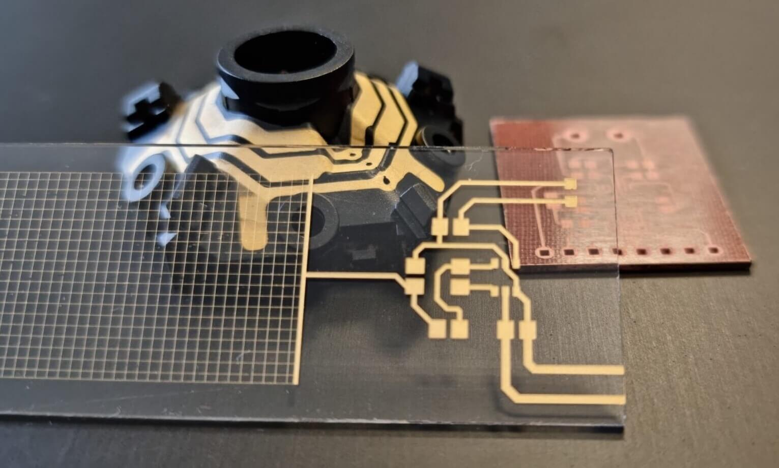
With a patented SSAIL technology conductive traces can be formed on many standard dielectric materials (polymers, ceramics, glass, silicon). It enables tighter electronics packaging on flat or 3D surfaces (with traces down to 1 μm width), making antennas directly on/in parts and creating functional surfaces.
How does it work
SSAIL is a two-step process:
- Laser activation of the surface for traces. It is done by scanning the surface with a laser beam.
- After the laser activation, the part goes through a chemical process:
- Chemical activation is done with a special solution, which prepares laser-activated areas for electroless plating.
- Electroless plating with copper and passivation layers (nickel, silver, gold).
Flexibility of shapes
Using SSAIL technology electrical traces can be used on different types of parts:
- 3D surfaces
- Thin films
- Flexible materials
- Through via plating
On most materials, a trace width of 15 µm can be achieved (down to 1 μm on some materials). Areas of square centimeters can be activated fast.
Materials
The technology works on many different dielectric materials, some of them include PC/ABS, PPS, Getinax, PA6, PF, FR-4, PVC, PI, Epoxy, PMMA, PC/ABS for 3D printing, RO3003TM Laminates, PE, PTFE, SITAL ceramic, PEEK, ABF, Al2O3 ceramic, PPA, PA4, Glass (soda lime), LCP, PBS, Fused Silica, PBT, PREP 200, Silicon
Applications
Once we talk about SSAIL technology main interest is coming from various developers (R&D labs) and electronic component producers. SSAIL could be used in the production of antenna modules, consumer electronics including touchscreens, automotive industry, glass heating or defrosting (defogging), local heating of the samples in scientific labs, etc.